PCB Design and Fabrication with NextPCB

The printed circuit board (PCB) is at the center of nearly all electronics products in the 20th century. PCBs originally consisted of wires placed along paths connecting a series of components on a rigid board — these were deemed printed wiring boards. Eventually, the printed wiring board morphed into the circuit boards with conducting strips etched into multi-layer boards that we see on PCBs today. The PCB industry is associated with nearly $1 trillion in sales of electronics each year [read more at: "Printed circuit board industry"]. Thus, it is important for engineers to know at least the basics of PCB design, even if the manufacturing is outsourced to companies. In this tutorial, we will introduce the design of a simple PCB and the process required to get the PCB manufactured by a company called NextPCB. Their process is simple and easy, and even allows the engineer to view their design on their online gerber file viewer.
The PCB will first need to be designed with a software tool. Once the PCB is designed, we need to save it and format it such that a manufacturer can read the file format and print the circuit board using their own software. We chose Fritzing due to its connection to Raspberry Pi and Arduino and the multitude of parts and components available within its libraries. The
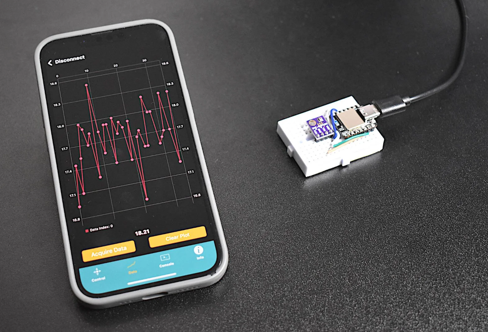
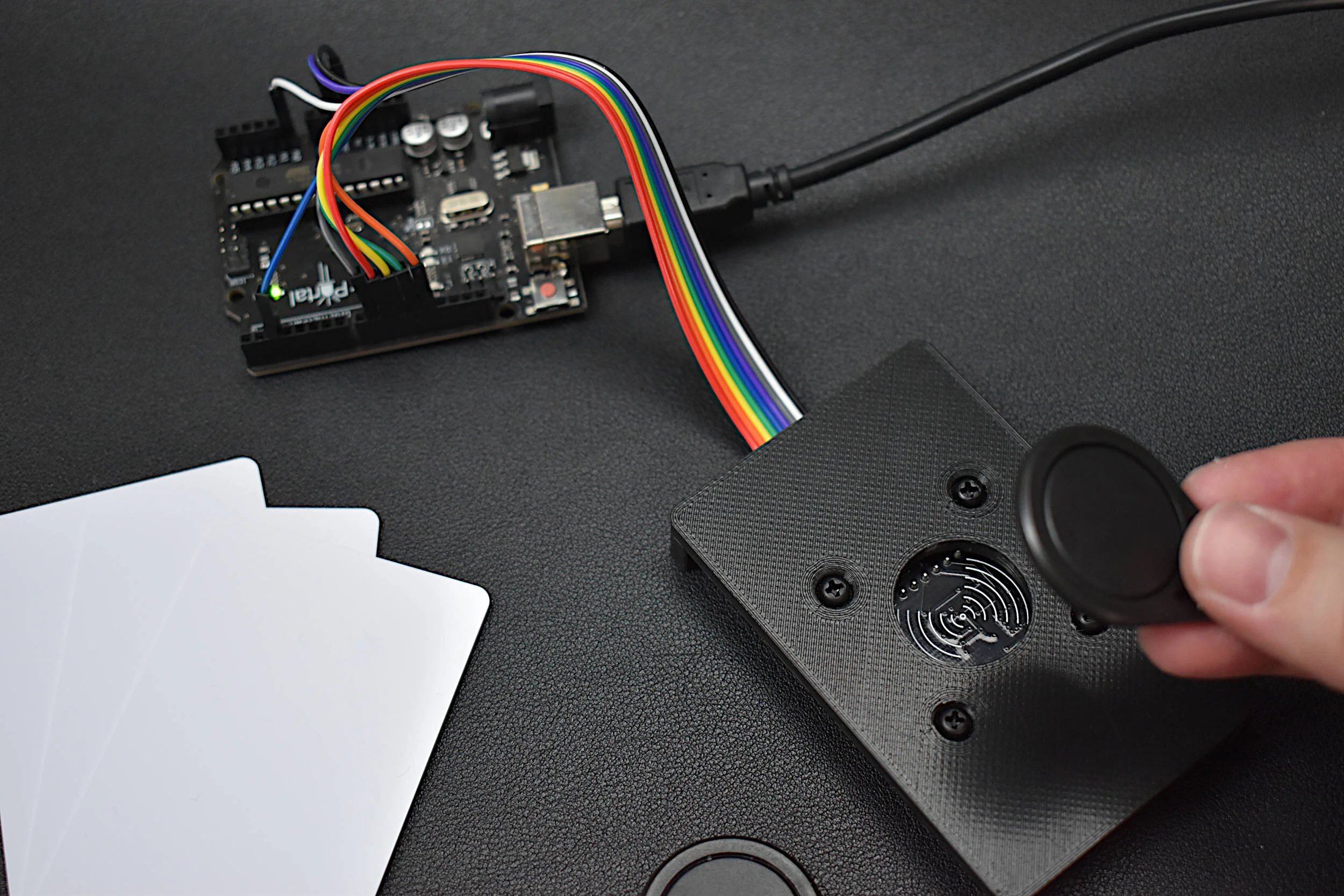
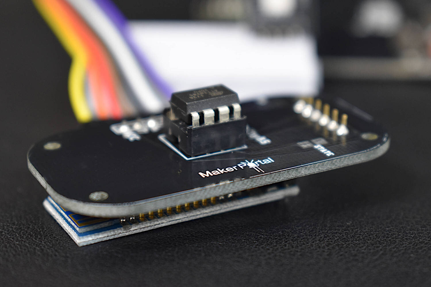
For this tutorial, we will be designing a simple PCB that houses an ATtiny85 and connector pin for a Bluetooth Low Energy (BLE) module, which is based on one of our previous tutorials that reads a temperature and humidity sensor and transmits the data via Bluetooth Low Energy to an iPhone using the BLExAR iOS app.

Fritzing is an open-source PCB design software
1. First, download the Fritzing software for your OS:
2. Next, open Fritzing and navigate to the PCB tab:

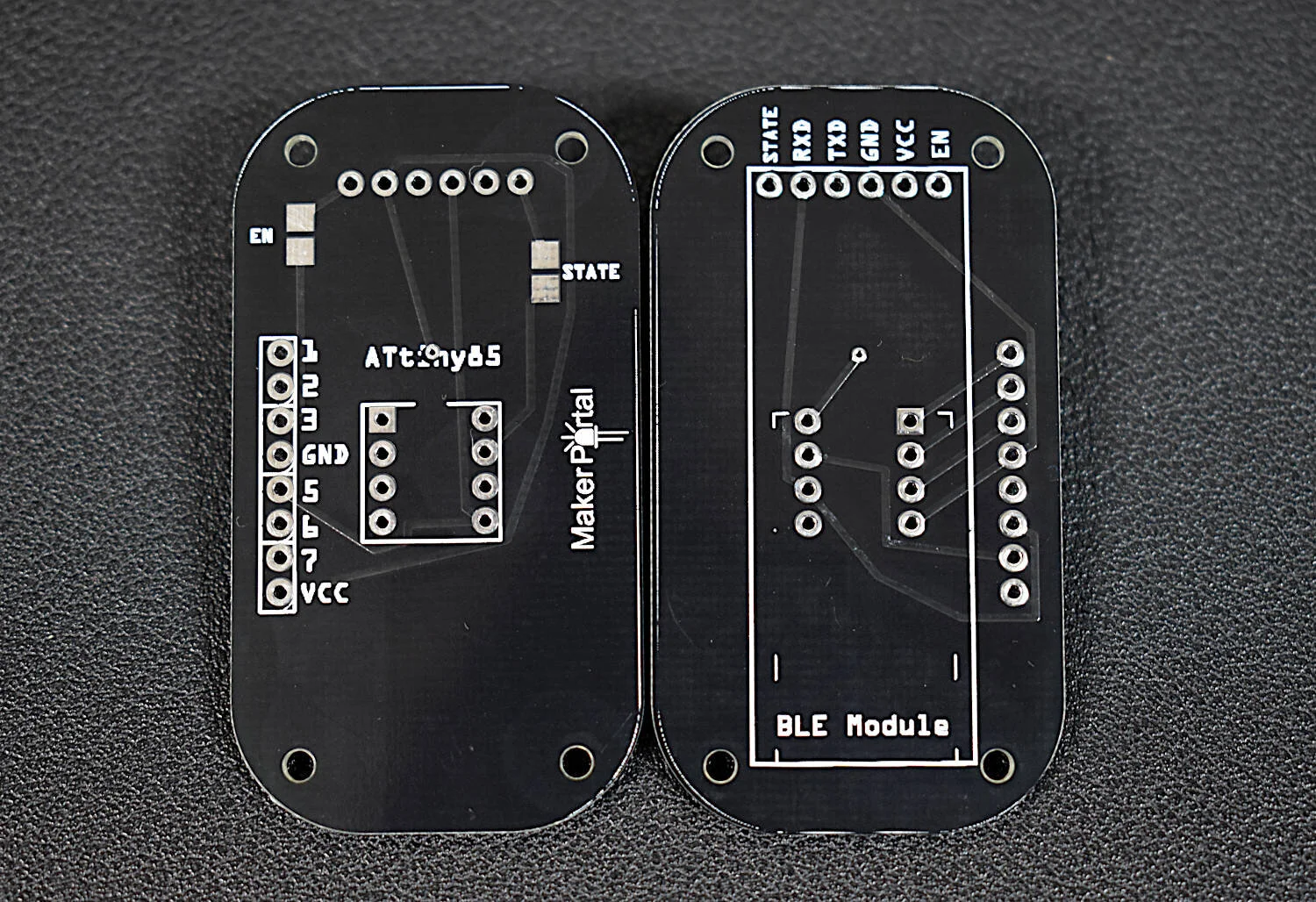
3. Next, we need to add our components such that we can create space for them on the PCB. In our case, we have added the ATtiny85 and an HC-05 Bluetooth module (which has the same footprint as the HM-10 - which we will be using):

4. Decide how you want to connect to the board and add the headers or connectors related to that connection. In our case, we are electing to add an 6-pin 2.54mm header which can be used to solder pin headers or JST-XH connectors. It might be useful to place holes for mounting. And finally, add silkscreen text to allow users (or assmeblers) to identify pin and component orientations, as well as identification of each PCB. Our final Pre-routing PCB is shown below:

PCB Designed with Fritzing Before Adding Connections
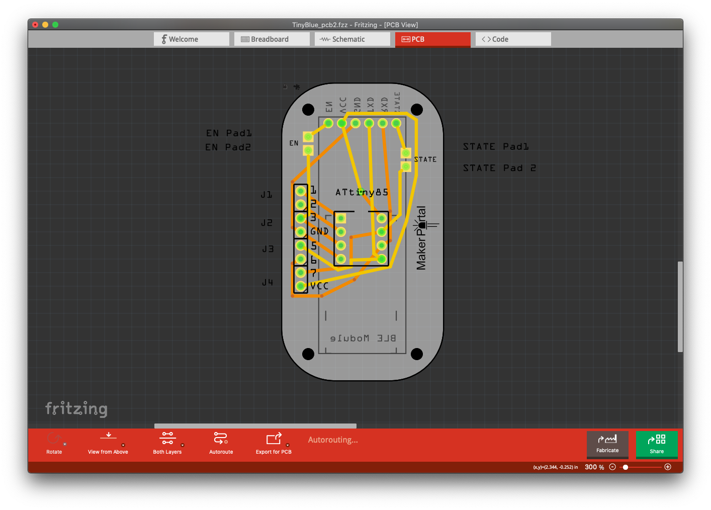
5. Finally, we need to add the connections and make sure the PCB is routed. Fritzing makes this very easy by allowing users to drag connections onto components. Below is our PCB with the connections added between the ATtiny85, HM-10 Module, and pin headers:
In the next section, we will introduce methods for viewing the PCB and uploading it to a PCB manufacturer, NextPCB.
NextPCB was founded in 2004 and has since established itself as a turnkey PCB manufacturing and assembly factory for prototyping quantities as well as small-volume to large-scale production.
NextPCB provides one-stop services for PCB design and manufacturing, with professional practices fulfilling advanced requirements for even the most complex circuits. The company provides the rapid solutions for PCBs and assmebly of PCBs and components. Their quality assurance practices are also highly noteworthy. Below, we go through the process of getting the designed PCB above manufactured by NextPCB.
NextPCB provides a range of PCB manufacturing options, with capabilities encompassing PCB layers from single-layer to 20-layer designs! We will only be manufacturing a 2-layer PCB, so the capability of a 20-layer PCB is pretty impressive! Their board thicknesses also range from uber thin at 0.6mm to rigid and strong PCB thicknesses of 2.5mm.
How to Order on NextPCB:
First, we need to export our project on Fritzing, using the following process:
1. Export your PCB by selecting “Export for PCB” in the main PCB window in Fritzing:

2. Make sure to save the files to an empty folder, perhaps with the title ‘export’
3. Compress the files into a single .zip file under the name of the project, such as ‘ArduinoPrj.’ In our case, we are using the name ‘TinyBlue.’
4. Next, go to https://www.nextpcb.com/ and click on ‘Instant Quote’ on the menu bar. One on the quote page, click <+Upload File> and be sure to upload the .zip file:

The user should be able to observe the following update once the file loads:
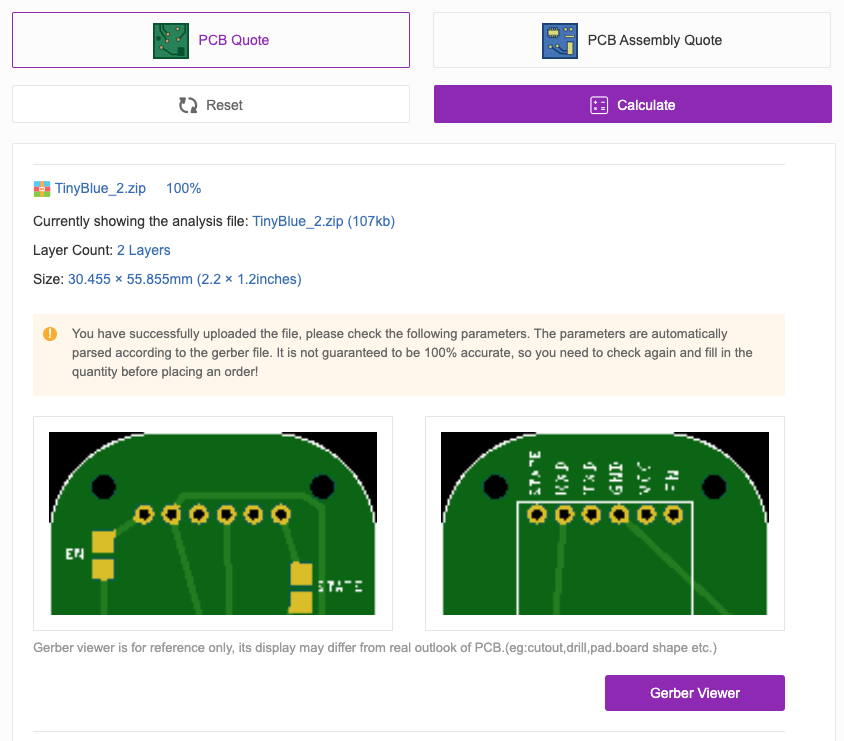
5. Continue to view the PCB by clicking on ‘Gerber Viewer’ which will allow the user to inspect the PCB’s layers:

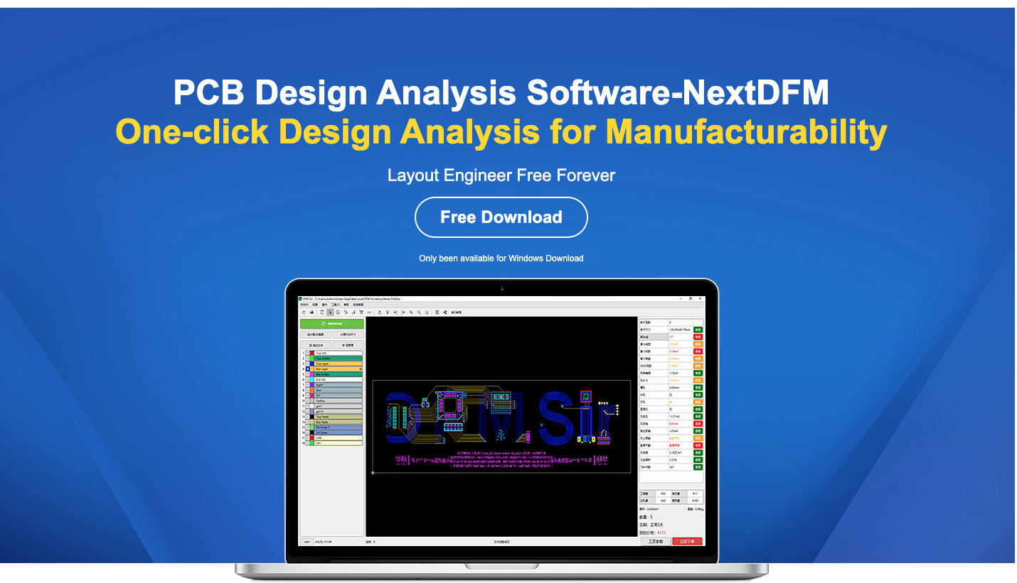
NextPCB also has a software tool called NextDFM that allows engineers to check their designs:

The NextDFM software has the following features for engineers:
Import the Gerber file with one click. It’s easy and simple.
The graphics are easy to read so you can make the file contains all necessary parts of your design.
NextDFM helps users become familiarized with DFM design specifications and production needs
Users can check whether there are hidden faults in their design files, they can select available parts, and evaluate the cost in real time.
It also provides precise control of the manufacturing details of surface-mount technology (SMT) and through-hole components.
A professional product and technical team is available to help users improve their design’s quality assurance, performance, and reliability.
It also lets you panelize your board — a crucial function missing from Eagle and KiCad.
NextDFM is an impressive software tool that is free for engineers! Check it out and download it at the link below:
6. To place your order for manufacturing, return to the Instant Quote page (and re-upload your gerber .zip file, if required). Next, ensure that all the variables on the PCB page are correct. These include the PCB color (we chose black for ours), PCB thickness (1.6mm is common), silkscreen color (white is best for most colors), and other selectable parameters. Most of the requirements are set by default, and are likely the best option for your application, if you are new to PCB design.
7. Once the quantity is inputted, the PCB manufacturing quote will be provided.
8. Finally, wait for the PCB to be accepted, continue with payment, and then wait for your PCB to arrive in the mail!

In this tutorial, we introduced PCB design with Fritzing and manufacturing with NextPCB. PCB design can be a useful asset for engineers that are not electrical or electronics engineers by trade, but are interested in custom electronics designs. This is why Fritzing was selected as the design tool. Furthermore, NextPCB makes taking PCB designs from software to manufacturing. NextPCB’s tools, such as their online gerber file viewer, or their NextDFM PCB inspector, are useful for perfecting an engineer’s design and taking it to production. They also have PCB assembly design options, which could take an idea from design to full production, by including assembly of parts in the manufacturing process.

Final PCB manufactured by NextPCB
See More in PCBs and Electronics: