PCB Design and Fabrication with NextPCB
The printed circuit board (PCB) is at the center of nearly all electronics products in the 20th century. PCBs originally consisted of wires placed along paths connecting a series of components on a rigid board — these were deemed printed wiring boards. Eventually, the printed wiring board morphed into the circuit boards with conducting strips etched into multi-layer boards that we see on PCBs today. The PCB industry is associated with nearly $1 trillion in sales of electronics each year [read more at: "Printed circuit board industry"]. Thus, it is important for engineers to know at least the basics of PCB design, even if the manufacturing is outsourced to companies. In this tutorial, we will introduce the design of a simple PCB and the process required to get the PCB manufactured by a company called NextPCB. Their process is simple and easy, and even allows the engineer to view their design on their online gerber file viewer.
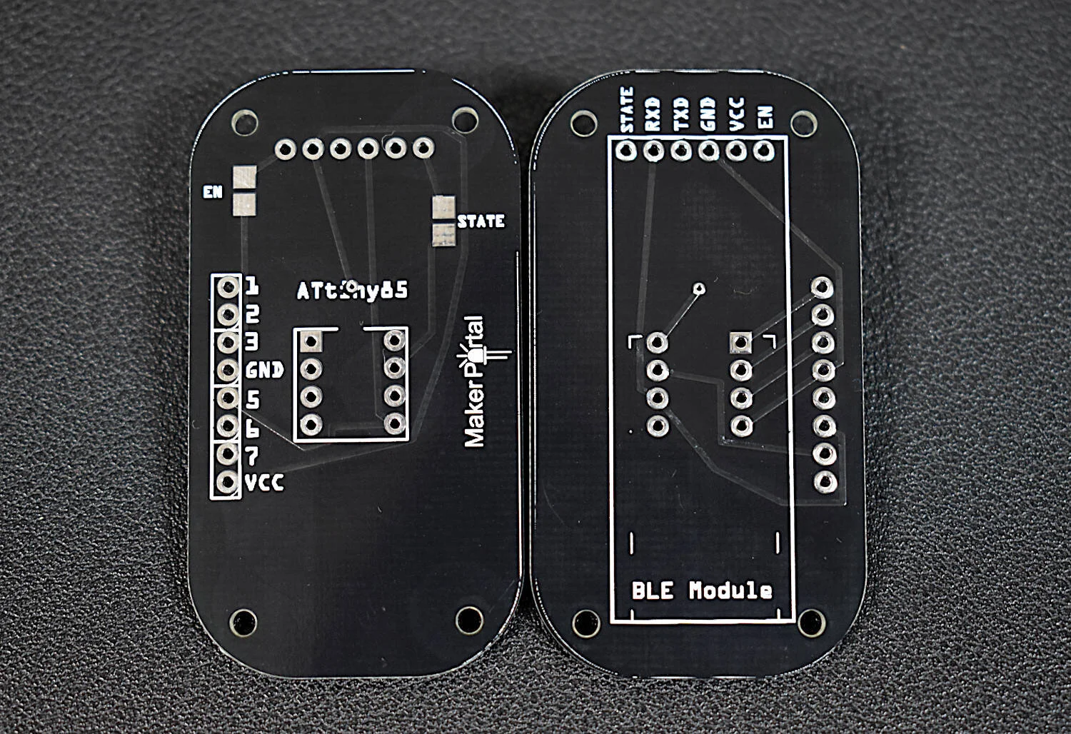
Importance of Silkscreens for PCB Identification and Labeling
Just as the signal lights of your car help to indicate when your car plans to take a turn or change lanes, the silkscreen is also used in the PCB process to help in testing and troubleshooting the board. The layer of silkscreen contains information regarding the PCB assembly process. This includes the location of components, their polarity and details for their placement and orientation, identifiers, labels and logos for various components. Your silkscreen must have a clear and readable font. In order to explain why silkscreen is so crucial let us discuss its importance in assembly and testing of PCBs.